
| Home |
| Dragonnorth... |
| Modules |
| Published Source License |
| Screen Shots |
| SD Card Issues |
| Updating Firmware |
| Reference Information |
| Airflow Setup |
| Development Environment |
| I2C Addresses |
| Module Switches Setup |
| MQTT |
| LOGGER Setup |
| Processor Module Pinning |
| WattNode Modbus Adapter |
| Development History |
| Breadboard |
| Project Status |
| Software Revisions |
References
| PJRC hardware |
| ESP8266 Information |
Processor Module Pinning
In this table the pinning listed in the PJRC Teensy, PJRC SD small and Wireless Sensors colums supports a number of development boards. These columns are not important for the Logger Developers Kit.
NOTE: pins on the large PJRC USB module are listed in the table as Teensy The pin numbers indicated are the "Digital Pins" printed on the Teensy card in grey. (These do not count around the card the way a DIP does.)
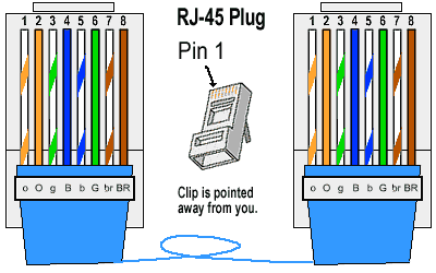
| Function | ESP pin | Cat-5 | SD adapter | PJRC Teensy |
PJRC SD small |
Wireless Sensors |
|---|---|---|---|---|---|---|
| Enable I/O Devices (turns on voltage regulators) | 1 White/Orange | Reset,
Power for Sensirion (SHT10 pin 5) |
||||
| SCL (ESP pullup expected) | GPIO2 on ESP8266
GPIO22 on ESP32 |
2 Orange | SCL for Sensirion (SHT10 pin 6),
Power for Onewire Temperature |
|||
Data Ready |
GPIO5 | 3 White/Green | ||||
| OneWire Data | GPIO0 | 4 Blue | SDA for Sensirion (SHT10 pin 1),
Data for Onewire Temperature |
|||
| GND | GND | 5 White/Blue | 3, 6 | GND (also AGND?) | GND (SHT10 pin 2) | |
| spare | 6 Green | |||||
| +5V | to Voltage Regulator then to 3.3V | 7 White/Brown | pin 4 does not connect to the Cat-5, it gets locally regulated 3.3V | |||
| SDA (pullup required) | GPIO4 on ESP8266
GPIO21 on ESP32 |
8 Brown | ||||
| SS (not chip select) | GPIO17 on ESP32 (GPIO10 is missing on SparkFun Thing)
GPIO10 on ESP8266 (pin 16 was used on older modules used for reset) |
1 | Teensy 4 | |||
| MOSI | GPIO13 | 2 | Teensy 11 | |||
| SCK | GPIO14 | 5 | Teensy 13 | |||
| MISO | GPIO12 | 7 | Teensy 12 | |||
| Analog Input | A |
Cat-5
SD Card
Soldering wires to pins 1 thru 7 of an SD card adaptor works without modification.
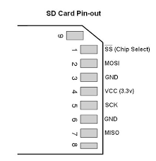
The first line is the end of the adapter with the notch. Pin 9 at this end is displaced from the edge. Yes the numbering is not in order.
| Pin # | Function |
|---|---|
| 9 | unused |
| 1 | SS (not chip select) |
| 2 | MOSI |
| 3 | GND |
| 4 | VCC (+3.3V) |
| 5 | SCK |
| 6 | GND |
| 7 | MISO |
| 8 | unused |
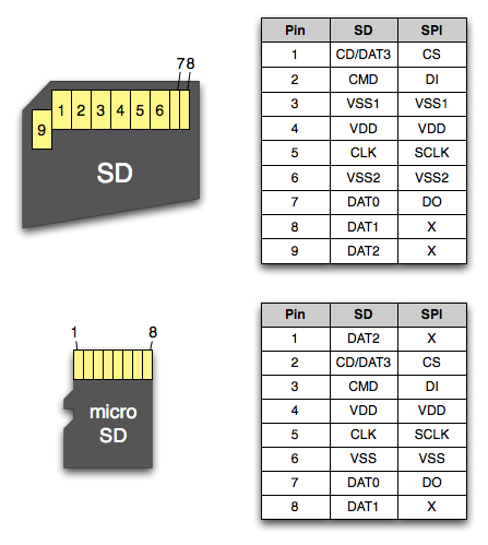
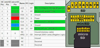
| Pin # | Pin name | SD Signal Function SD Mode | SPI Signal Function SPI Mode |
| 1 | DAT3/CS | Data Line 3 | Chip Select/Slave Select [SS] |
| 2 | CMD/DI | Command Line | Master Out/Slave In [MOSI] |
| 3 | VSS1 | Ground | Ground |
| 4 | Vdd | Voltage Supply [2.7v or 3.6v] | Voltage Supply [2.7v or 3.6v] |
| 5 | Clock | Clock | Clock [SCK] |
| 6 | Vss2 | Ground | Ground |
| 7 | DAT0/D0 | Data Line 0 | Master In Slave Out [MISO] |
| 8 | DAT1/IRQ | Data Line 1 | Unused or IRQ |
| 9 | DAT2/NC | Data Line 2 | Unused |
Cables and Parts
Adafruit Selectable programming Module (Recommended programmer can be selected for 3.3V or 5V operation)Adafruit Serial programming cable
Breakout Boards
1230 moduleOther Breakouts
Large PJRC SD Adaptor
The PJRC Rev1 SD adaptor works without modification. The Rev2 SD adapter adds pullup resistors which are in conflict with the processor pin usage and must be removed if the Rev2 adaptor is used.
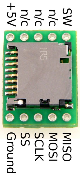
Small PJRC SD Adaptor
The Small PJRC SD Adaptor works without modification. The jumper for 3.3 Volt operation must be installed. The 5 Volt pin then becomes the 3.3 Volt input. The SS pin on this module interferes with normal boot of an ESP8266 when it is connected to pin 15. The SD card chip select has been moved to pin 16 to avoid this issue.
Modules Available
Sparkfun FTDI equivalentWhile the Raspberry Pi module is cheaper it does not do the FTDI thing, and anything but an authentic FTDI chipset is a recipe for great pain according to the ESP8266 blog. Sparkfun FTDI equivalent
Newer parts ESP-12F are availableInterfacing a LOGGER to a Wattnode Modbus meter
To connect a LOGGER to a WattNode Modbus meter an external modbus transceiver interface is necessary. The first table below shows how to connect a LOGGER Cat-5 connector to a MAX3485 RS485 to Modbus transceiver. The second table shows how to connect the transceiver to the 4 pin Com port of the Wattnode Modbus meter.
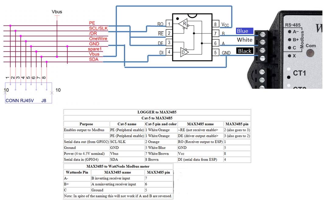
| LOGGER to MAX3485 | ||||
|---|---|---|---|---|
| Cat-5 to MAX3485 | ||||
| Purpose | Cat-5 name | Cat-5 pin and color | MAX3485 name | MAX3485 pin |
| Enables output to Modbus | PE (Peripheral enable) | 1 White/Orange | ~RE (not receiver enable> | 2 (also goes to 3) |
| PE (Peripheral enable) | 1 White/Orange | DE (driver output enable> | 3 (also goes to 2) | |
| Serial data out (from GPIO2) | SCL/SLK | 2 Orange | RO (Receiver output to ESP) | 1 |
| Ground | GND | 5 White/Blue | GND | 5 |
| Power (4 to 4.5V nominal) | Vbus | 7 White/Brown | Vcc | 8 |
| Serial data in (GPIO4) | SDA | 8 Brown | DI (serial data from ESP) | 4 |
| MAX3485 to WattNode Modbus meter | ||
|---|---|---|
| MAX3485 name | MAX3485 pin | Wattnode Pin |
| B inverting receiver input | 7 | A- |
| A noninverting receiver input | 6 | B+ |
| Ground | 5 | C |
| Note: In spite of the naming this will not work if A and B are reversed. | ||
| AllSensors E1NS package to Cat-5 | ||
|---|---|---|
| AllSensors Name | AllSensors pin | Cat-5 Pin |
| Gnd | 1 | 5 |
| Vs | 2 | 1 (+3.3 if insufficent current) |
| SDA | 3 | 8 |
| SCL | 4 | 2 |
| Sparcfun Qwiic to Cat-5 | ||
|---|---|---|
| Sparcfun Name | Sparcfun pin | Cat-5 Pin |
| Gnd (black) | 1 | 5 white/blue |
| Vs (red) | 2 | 6 green (this spare pin must be tied to +3.3 at P1 or P2 on processor board) |
| SDA (blue) | 3 | 8 brown |
| SCL (yellow) | 4 | 2 orange |
Send comments and corrections to:
Webmaster: mnewman@dragonnorth.com